Enjoying this issue?
Get tomorrow's AI & engineering digest in your inbox — hand-picked, summarized, and always spam-free.
TLDR
Xiaomi's X-Ring O100 chip achieves 1.22 TB/s memory bandwidth by using wafer-on-wafer hybrid bonding at a 1.4 micron pitch, creating 28,672 data lines between memory and compute—a 300x increase over conventional phone packages. This is the real story behind the AI Cube, not the box itself. The packaging decision trades yield during a memory shortage for bandwidth, and the chip's on-chip network switches between ring and broadcast topologies depending on the inference phase. The viral spec list of 200 TOPS, 160 GB unified memory, and 330 tokens/s came from combining figures from three different Xiaomi chips, not the O100 alone.
Key points
Xiaomi demonstrated an AI cube running a 120B parameter model locally using three chips: O3, O100, and D100, each with different specs.
The O100 achieves 1.22 TB/s memory bandwidth via wafer-on-wafer hybrid bonding with 1.4 micron pitch, compared to TSMC's ~6 micron and HBM4's ~10 micron microbumps.
Hybrid bonding creates 28,672 data lines (300x increase over a phone's 96) by stacking memory wafers directly onto a compute wafer with copper-to-copper fusion.
Wafer-on-wafer bonding scraps entire wafers if a single die is defective, making yield costly—especially during a memory shortage where prices rose 400% from 2024-2025.
The O100 includes an on-chip network that switches from ring topology (for prefill) to broadcast topology (for decode/auto-regressive generation), optimizing both phases.
The 330 tokens/s headline figure came from a lab test on the 3B-parameter Mimo model, not the 120B model, and the 200 TOPS and 160 GB unified memory belong to the O3 and D100 chips respectively.
Xiaomi's fast-slow system switching runs a small model from fast memory instantly and a larger 120B model from LPDDR6 memory only when needed, using the O100 as a co-processor.
The O100 is designed for a 10-watt thermal envelope, targeting phones, PCs, robots, and cars, rather than being a desktop DGX Spark competitor.
Tools mentioned
Techniques
- wafer-on-wafer hybrid bonding
- 1.4 micron pitch bonding
- 28,672 effective data lines via through-silicon vias
- on-chip network with ring/broadcast topology switching
- fast-slow system switching
Stop scrolling. Start reading smarter.
Receive the day's most important AI & engineering updates in one concise email. No spam.
Transcript (captions)
Xiaomi just set a small aluminium cube on a table in Beijing. No cloud behind it. Everything running on the box itself. On it, they ran a model with 120 billion parameters, three chips inside,
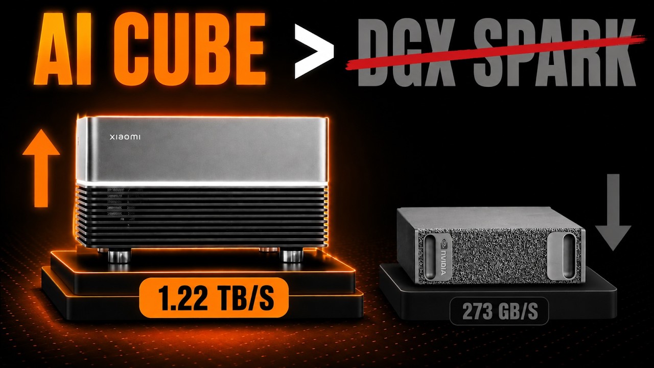
every one of Xiaomi's own design. And one number on the slide stopped the room. 1.22 tab a second of memory bandwidth. For scale, take Nvidia's DGX Spark, the desktop AI box developers
have been buying all year. It moves 273 GB a second. So Xiaomi's figure is 4 and a half times that at 150 watts from a company whose first 3 nanometer chip is 15 months old. The timelines already
have a name for it. China's DGX Spark. You've probably seen that post. That framing is wrong. And it's wrong in a way more interesting than the compliment it was meant to be because the cube
isn't the story at all. Xiaomi's own slide has the word prototype printed on it and no price or date came with it. The story is the middle chip. It's the X-Ring0100
and it's built on a 6nanmter process. 6 nanmters is old. Your phone from 5 years ago was 6 nm. That node shouldn't do this. So where does the bandwidth come from? Not from the transistors. It comes
from a packaging decision most of the industry has looked at and refused to make. And once you see what Xiaomi gave up to get it, the whole announcement reads differently. Start with the
problem because the number only means something once you know what it's fighting. When a model generates text, it's memory bound. to produce one token. It reads the weights it needs out of
memory, does a little arithmetic, writes one answer back, repeats. The arithmetic isn't the bottleneck, the reading is. So, the ceiling on how fast a model talks to you isn't operations per
second. It's bytes per second dragged out of memory into the compute cores. That's the memory wall, and phones hit it hardest. In a phone, memory sits on top of the processor in a package on
package stack, and the two talk through a ring of solder balls around the edge. Xiaomi's own figure for how many data connections that gives you is 96. 96 wires for everything a language model
needs. So the O00 does something different. Instead of stacking two finished chips and wiring them at the edge, Xiaomi takes the memory wafer and the compute wafer whole wafers before
anyone cuts them into chips and bonds them face to face. Two layers of memory on one layer of a 14 core neural processor. The industry calls it wafer on wafer. And to join them, Xiaomi
didn't use solder. This is the part that matters. Conventional stacking uses micro bumps, tiny solder balls, and even in the high bandwidth memory shipping today, those bumps sit tens of microns
apart. Xiaomi used hybrid bonding instead. Copper pads on one wafer pressed directly onto copper pads on the other and fused. No solder, no gap. The pitch Xiaomi claims is 1.4 microns. Read
that against the industry and it's an aggressive number. TSMC's production stacking, the technology it uses to bond cache memory onto processors, runs at about 6 microns, HBM four. The memory
going into cloud accelerators right now looked at hybrid bonding and stayed on microbumps near 10 because the economics didn't justify the move. Xiaomi's own slide says the quiet part out loud. On
bonding pitch, they claim to be ahead of the memory inside cloud AI chips. On that one metric, the public numbers agree with them. Here's what it buys. 2.58 million bonding points between the
wafers through silicon via the vertical holes carrying signal up through a wafer at 0.7 microns across. Xiaomi calls the result data wells, short vertical shafts dropping straight into the compute cores
instead of a path that runs out to the edge of a die and back, which brings us to the number the headline was built on. All of it adds up to 28,672 effective data lines between memory and
processor against 96 in a normal phone package. roughly a 300 times increase in data paths. And that's the entire explanation for the headline. Xiaomi didn't make the memory faster. They made
the road 300 times wider. So that's the packaging. If it's this good, why isn't the rest of the industry doing it? Because Xiaomi paid a price for it that most companies won't. Wafer on wafer has
a hard rule. You bond entire wafers before anyone cuts them. So you can't choose which ones to use. Die to wafer bonding lets you test first and bond only the good ones. known good die the
industry calls it wafer on wafer doesn't a perfect memory die landing on a defective processor die is scrap and your yield is roughly one wafer's yield multiplied by the others which is why
the technology lives where it does Sony has stacked camera sensors this way for over a decade and Chinese memory maker YMTC builds its flash the same way both stack simple regular high yielding
layers Xiaomi is doing it with a 14 core neural engine which is neither and look at the timing JP P Morgan's research team estimates memory prices will have risen more than 400% between the start
of 2024 and the end of this year. SKH says it is sold out through this year and Xiaomi isn't watching from outside. On its last earnings call, it named memory costs as the reason its phone
gross margin fell to 8 12%. Scrapping good memory wafers because the logic underneath failed is expensive in a normal year. In this one, it's a statement. Xiaomi is spending yield, the
scarcest thing in the industry to buy bandwidth. Now, the second half of the engineering, and this is the detail that made me want to cover the chip instead of the box. Getting bytes to the edge of
the compute wafer is only half the job. You've still got to move them between 14 cores. Xiaomi built its own onchip network for that. A high bandwidth matrix bus and it changes shape while
the model is running. When you send a prompt, the model reads all of it at once and builds up its internal state. That phase is called prefill and it's predictable. Data flows from one stage
to the next in order. So the bus runs as a ring. Each core handing off to its neighbor. Then generation starts and the work inverts. Now the model makes one token at a time and every core needs the
same freshly written state before the next token can begin. A ring is wrong for that. You'd sit waiting while data walk the loop. So the bus switches to broadcast. One right. Every core sees
it. Ring for prefill. broadcast for decode. Same silicon, two topologies picked by which half of inference you're in. I went through the launch coverage on this chip and outside Xiaomi's own
materials, the English write-ups I found don't mention it. It's the most thoughtful thing on the slide. So that is the chip. Two things so far. The packaging is real and the road into the
cores is 300 times wider. Then why did almost every writeup get the machine wrong? Because of the exact habit this channel keeps arguing against. And here it produced four errors inside one spec
list. Let me take that viral post line by line and I want to be fair. Every figure in it is a real Xiaomi number. The problem is which chip each one belongs to. 200 tops of AI compute real
and it's the O3, the phone chip shipping next month in the Xiaomi 18fold. Xiaomi published no tops figure for the O00 at all. Up to 160 GB of unified memory. also real and it belongs to the D100, a
3nm self-driving chip, a spec sheet maximum, not a machine anyone was shown. 1.22 TB a second real and it is the 0. But read Xiaomi's own wording near memory bandwidth. That's the speed
between the compute wafer and the two memory wafers bonded to it. And Xiaomi has not said how big that stacked memory is. Not in the release, not in the Chinese technical coverage, not anywhere
I could find, which matters more than anything else here. That model squeezed down to four bits is roughly 60 gigabytes. No chance that fits on two memory wafers. So, the big model isn't
in the fast memory at all. It's an LPDDR6, the new low power standard this cube is among the first compact systems to use. Xiaomi published no bandwidth figure for the D100's memory. And the
only LPDDR6 number on any of the three chips is the 03s. 113 GB a second, 113, not 1,220. Then 330 tokens a second. The figure in every headline, Xiaomi's Chinese
materials say exactly where it came from. A lab test on Mimo 3B, their own 3 billion parameter model. 3 billion, not 120. For scale, a DGX Spark running an open model of that bigger class
generates 46 to 60 tokens a second, depending on your kernel. Community benchmarks in the llama.cpp repository on hardware you can buy today. Xiaomi's 330 and Nvidia's 46 aren't the same
measurement. To be fair to Xiaomi, the O3 earns its own mention here. 3 nanmters, 10 cores with no small ones among them, and a multi-core score in the 15,000s. The review channel
Geekerwan measured its efficiency curve against Apples and called it alien technology. None of which makes Xiaomi dishonest. Every number is attributed correctly on their own slides. The
arithmetic happened afterwards when three chips best figures got added up and printed as one machine. And Xiaomi told us the real design if you read the demo instead of the slide. The cube ran
a 120 billion model and a 3 billion model together with what they call fast slow system switching. The small one answers instantly out of fast memory. The big one wakes up when the question
is hard. That isn't a workound. That's the architecture. At this point, the box has lost most of its headline. So, if the cube can't be your desktop AI machine, what is it for? Here, the story
gets bigger than the hardware. And it explains why Xiaomi built this and Nvidia wouldn't. Xiaomi doesn't sell developer workstations. What it sells is more than a billion connected devices
that count on its own platform at the end of June from its quarterly filing. Its voice assistant has 175 million monthly users. It makes electric cars. Its factory robots are already on a
third generation. Read the 0100 against that and it changes shape. It isn't a desktop part. It's a co-processor. Xiaomi's technical writeup describes a 10 watt class thermal envelope. An old
cheap node sitting beside a main chip doing one job, feeding a language model fast enough to feel instant. Xiaomi's materials list where it's headed. phones, PCs, robots, cars. The founder,
Lelay Jun, put it plainly on launch day. X-ring, he wrote, is the physical foundation of Xiaomi's AI strategy, not only its chip strategy. He'd promised his team a decade of it and 50 billion
yuan. 5 years in, they are not yet halfway through that budget with a chip team in the thousands. And there's an irony inside all of it. Xiaomi's own flagship models are far too big for
Xiaomi's own box. MIMO 2.5 is over 300 billion parameters and the Pro version is over a trillion. Both sit on hugging face under an MIT license. Neither fits what Xiaomi showed. Even the D100's own
spec sheet tops out just above 200 billion, which tells you what the demo was proving. Not that you'd run Frontier models at home, that the class of model people rent by the token can be made to
sit on a shelf and run on wall power. Whether that's your shelf or your car's dashboard is a packaging problem now. So, price and dates since that's the first thing in every reply under that
post. Xiaomi announced neither for the Cube, and I'd be careful assuming it becomes a product at all. The chips have a date. The O00 and D100 are finished and go commercial next year. The O3 is
already in mass production, launching next month in a foldable that Chinese reporting puts above 10,000 yuan. If a cube ever ships, here are the anchors worth using. A DGX Spark is about $4,000
for the Founders Edition and several hundred more through partners. Xiaomi has a long-standing public pledge capping hardware net margin at 5% and a long record of undercutting its rivals.
Put those together and you'd expect a Xiaomi box under Nvidia's, but that's a guess from Xiaomi's history, not a number anyone has published. How far under depends on memory prices next
year, and no analyst I read will forecast those. So, here's the verdict, and it isn't the one the headline promised. two halves and they pull opposite ways. The AI Cube isn't a DGX
Spark competitor and probably never will be. If you want a 120 billion parameter model on your desk this year, buy the Nvidia box. It exists, it ships, it runs CUDA, and its slower memory is attached
to the whole pool instead of an undisclosed slice. That's the concession, and it's real. But the O00 is the more important chip. And I'd say that even if the cube never ships, it's
a working answer to the question every ondevice AI team is stuck on. And the answer is packaging rather than lithography. A six nanometer part outrunning Nvidia's box on memory
bandwidth is the clearest evidence yet that the gains moved from how small you can print to how tightly you can stack. That's thesis 4 on this channel and it keeps paying. Local capability compounds
the hardware floor keeps dropping. What's new is where the drop came from. Not a node, a bond. And the villain is the usual one in a new outfit, not benchmark worship this time. Spec sheet
arithmetic. Three chips best numbers added up, printed as one machine, repeated by writers who didn't check which chip owned which figure. Here's the question I'd leave you with because
I don't have a confident answer. Xiaomi bought this bandwidth by giving up the ability to throw bad dies away in the middle of a memory shortage. If those yields hold, wafer on wafer gets copied
fast and every phone chip in 2028 looks like this. If they don't, the 0100 is a beautiful prototype the yield maths won't allow. So which is it? A crack in the memory wall or the one place a
company with a billion devices can afford to spend yield.